Interface implementation details that look right at a glance
Some of the hardest schematic issues to catch are not obviously broken connections. They are interface details that appear reasonable on the page, but do not match how the circuit should actually behave. These problems often hide inside otherwise familiar signal paths, where reviewers recognize the pattern, trust what they are seeing, and move on quickly.
What this can look like:
A termination resistor is placed on the wrong side of an interface.
Biasing or pull resistors suggest an operating mode the design did not intend.
A familiar high-speed or differential pair is wired in a way that does not match the signaling standard.
One instance of a repeated interface block differs subtly from the rest of the design.
Why it happens
These issues are easy to miss because they often combine familiar parts, familiar net names, and familiar topologies. The reviewer may understand the interface well and still miss one detail that changes how the circuit behaves in practice.
The operational cost
When interface implementation details escape review, the result is often long debug sessions, signal integrity problems, or inconsistent behavior that only shows up during validation and bring-up.
A line termination that does not match the interface design
One useful example is a resistor that looks reasonable in isolation, but does not match how the interface should actually be terminated.
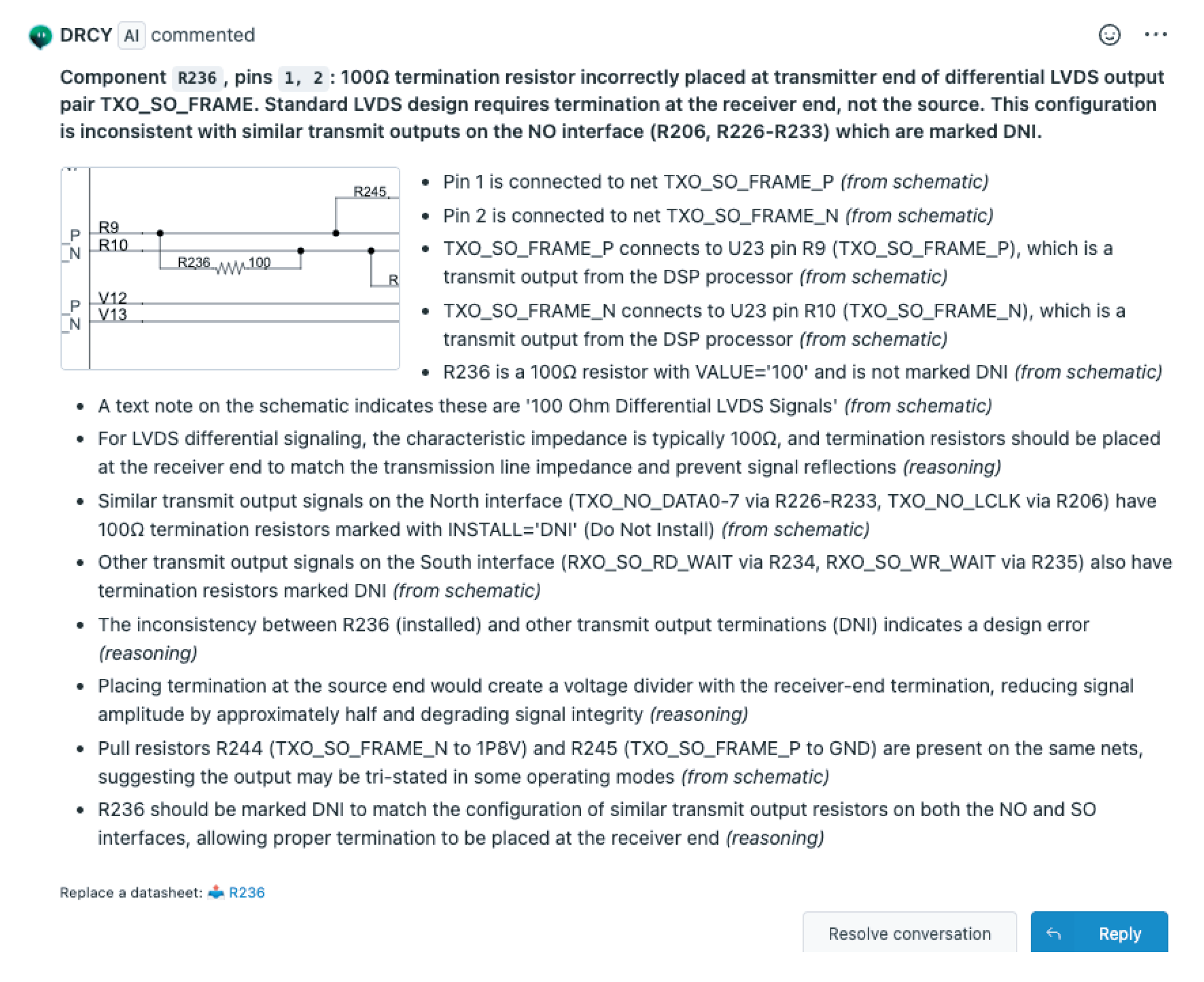
In this DRCY finding, the system flagged resistor `R236` and explained that a 100 ohm termination resistor had been placed at the transmitter end of a differential LVDS output pair instead of at the receiver end. What makes this example useful is that the schematic still looks tidy at a glance. The resistor value is familiar. The nets are named clearly. Nothing about the symbol itself looks obviously wrong. But the electrical context tells a different story.
DRCY did not stop at pointing to the part. It showed why the placement was suspicious:
- `R236` was connected across the `TXO_SO_FRAME_P` and `TXO_SO_FRAME_N` nets at the transmit side.
- The schematic note identified the signals as 100 ohm differential LVDS.
- Similar transmit output terminations elsewhere in the design were marked DNI.
- That inconsistency suggested this resistor was not meant to be installed in this location.
The reasoning also matters. For LVDS interfaces, termination is typically placed at the receiver so the line impedance is matched at the point where the signal is received. Placing the resistor at the source can degrade signal integrity and create behavior that is harder to debug later. This is exactly the kind of issue that can slip through manual review. A reviewer may see a familiar resistor value on familiar nets and move on. A first-pass review layer is useful because it can compare the local circuit pattern against the broader design and highlight where one instance does not match the rest.
How AI-assisted reviews help
AI can help compare interface patterns across the design, check whether supporting circuitry matches the expected signaling scheme, and flag cases where one block does not align with the surrounding context or datasheet guidance.
For managers, this matters because it reduces the odds that a small schematic detail turns into a larger validation or bring-up delay. Not every costly escape begins with a connection or package problem. Some of the most persistent downstream friction starts with the design data surrounding the circuit.